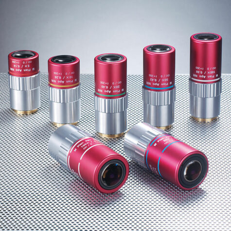

Mitutoyo LCD Plan Apo NIR & NIR HR Objectives (20x–100x) – Infrared-Optimized, Long Working Distance Optics
$4,520.00 – $16,400.00The Mitutoyo LCD Plan Apo NIR and NIR HR series deliver outstanding performance across the near-infrared (NIR) spectrum, optimized for inspection, metrology, and failure analysis in silicon, MEMS, and other IR-transparent materials. Covering magnifications from 20x to 100x, these objectives provide high numerical apertures, long working distances, and minimal aberration—making them ideal for laser-based alignment, backside wafer inspection, and biological IR imaging.
The HR (High Resolution) variants push the limits of clarity and detail, especially at 50x and 100x, offering sharper, more contrast-rich imaging while maintaining infrared compatibility. Whether you’re working with IR lasers, spectroscopy setups, or NIR fluorescence, this series ensures precision and flexibility at every magnification.